Search results
Search for "ultrahigh vacuum" in Full Text gives 154 result(s) in Beilstein Journal of Nanotechnology.
Superconducting spin valve effect in Co/Pb/Co heterostructures with insulating interlayers
Beilstein J. Nanotechnol. 2024, 15, 457–464, doi:10.3762/bjnano.15.41

- the magnetization of the Co1 layer. The layers were deposited using electron beam evaporation (Co, Pb) and AC sputtering (Si3N4). The deposition setup had a load-lock station with vacuum shutters, allowing one to transfer the sample holder without breaking the ultrahigh vacuum in the deposition


![[Graphic 6]](/bjnano/content/inline/2190-4286-15-41-i6.svg?max-width=637&scale=1.18182)
Unveiling the nature of atomic defects in graphene on a metal surface
Beilstein J. Nanotechnol. 2024, 15, 416–425, doi:10.3762/bjnano.15.37

- of defects. Experimental A combined STM-AFM was operated in ultrahigh vacuum (5 × 10⁻⁹ Pa) and at low temperature (5 K). Surfaces of Ir(111) were cleaned by Ar+ ion bombardement and annealing. The epitaxial growth of graphene proceeded by exposing the heated (1300 K) Ir(111) surface to the gaseous


CdSe/ZnS quantum dots as a booster in the active layer of distributed ternary organic photovoltaics
Beilstein J. Nanotechnol. 2024, 15, 144–156, doi:10.3762/bjnano.15.14

- monocrystalline silicon. A WITec Alpha 300 M+ spectrometer with a 488 nm laser, 600 groove grating, and a 100× ZEISS objective was used for Raman measurements. The samples were deposited on a glass substrate. Ultraviolet photoelectron spectroscopy (UPS) was conducted in an ultrahigh-vacuum chamber with a base


unDrift: A versatile software for fast offline SPM image drift correction
Beilstein J. Nanotechnol. 2023, 14, 1225–1237, doi:10.3762/bjnano.14.101

- velocity. In Figure 4a,b, we show two consecutive AFM images of a calcium fluoride (111) surface recorded under ultrahigh vacuum conditions. The periodic structures observed in these two raw-data images (see red unit cells in Figure 4a,b) show a striking difference compared to each other and compared to
- optimized lattices as found by unDrift are shown as red lines. Only the centers of the autocorrelations are shown. (a, b) Two consecutive up images recorded with high-resolution AFM on calcite(10.4) in ultrahigh vacuum. The images show several defects, whose positions are marked with colored crosses in both
- the corresponding drift-corrected images are shown on the right side. In all images, the unit cell used for drift correction is shown as a red quadrangle. Images (a–d) show the atomic structure of calcium fluoride (111) recorded with high-resolution AFM in ultrahigh vacuum. Images (e–h) and (j–m) were


A combined gas-phase dissociative ionization, dissociative electron attachment and deposition study on the potential FEBID precursor [Au(CH3)2Cl]2
Beilstein J. Nanotechnol. 2023, 14, 1178–1199, doi:10.3762/bjnano.14.98

- composition and morphology of FEBID deposits fabricated in an ultrahigh-vacuum (UHV) chamber were explored on different surfaces and at varied beam currents. In the gas phase, dissociative ionization was found to lead to significant carbon loss from this precursor, and about 50% of the chlorine was on average
- ; quantum chemical calculation; ultrahigh vacuum; Introduction In recent years, gold nanostructures have received much attention owing to their dielectric properties [1], their biocompatibility [2], and their electrical properties [3][4], which enable a multitude of exciting applications in the field of
- . [26] under the term focused-electron-beam-induced mass spectrometry (FEBiMS). In this approach, ion-extraction mass spectrometry, in close proximity to the forming FEBID structure, is used to analyze the charged, desorbing ligand fragments. Another approach in this direction is to combine ultrahigh


Dual-heterodyne Kelvin probe force microscopy
Beilstein J. Nanotechnol. 2023, 14, 1068–1084, doi:10.3762/bjnano.14.88

- applications of KPFM are extremely broad. It is now used by physicists, chemists, and biologists to characterize the nanoscale electronic/electrostatic properties of an ever-expanding range of materials, interfaces, and devices, in ambient conditions, under ultrahigh vacuum, or at the liquid–substrate


Two-dimensional molecular networks at the solid/liquid interface and the role of alkyl chains in their building blocks
Beilstein J. Nanotechnol. 2023, 14, 872–892, doi:10.3762/bjnano.14.72

- flat conducting substrates, such as metal surfaces and highly oriented pyrolytic graphite (HOPG), under ultrahigh vacuum (UHV) conditions, at solid/air or solid/liquid interfaces [23][24][25][26][27][28]. Although UHV-STM offers high-resolution imaging, it requires large, complex, and expensive


N-Heterocyclic carbene-based gold etchants
Beilstein J. Nanotechnol. 2023, 14, 865–871, doi:10.3762/bjnano.14.71

- attachment of NHCs to gold and the properties of the corresponding monolayers have been studied using conventional surface science techniques under ultrahigh-vacuum conditions [13][14]. NHC monolayers have also been used in applications such as surface-enhanced Raman spectroscopy and surface plasmon


Cross-sectional Kelvin probe force microscopy on III–V epitaxial multilayer stacks: challenges and perspectives
Beilstein J. Nanotechnol. 2023, 14, 725–737, doi:10.3762/bjnano.14.59

- paragraph, KPFM measurements can be performed in ultrahigh vacuum (UHV) at an optimal surface–tip distance of the order of a few nanometres [34] with particular attention to the sample preparation either in the deoxidation and cleaving process. Effect of the illumination on the VCPD In the Results section


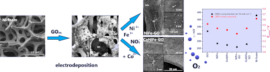
Evaluation of electrosynthesized reduced graphene oxide–Ni/Fe/Co-based (oxy)hydroxide catalysts towards the oxygen evolution reaction
Beilstein J. Nanotechnol. 2023, 14, 420–433, doi:10.3762/bjnano.14.34
- obtained on an ultrahigh vacuum spectrophotometer at a pressure below 1.1 × 10⁻⁸ mbar at room temperature (Omicron NanoTechnology). Photoelectrons were detected by a spectrophotometer equipped with a 128-channel collector. The X-ray anode was operated at 15 keV and 300 W. The chemical composition


Intermodal coupling spectroscopy of mechanical modes in microcantilevers
Beilstein J. Nanotechnol. 2023, 14, 123–132, doi:10.3762/bjnano.14.13

- coherent bimodal drive to amplify the signal of the fundamental mode. Both increase the signal-to-noise ratio of the measurement, creating opportunity for either improved sensitivity or increased speed. Furthermore, sideband cooling has a secondary use in ultrahigh-vacuum AFM as a tool for controlling the


From a free electron gas to confined states: A mixed island of PTCDA and copper phthalocyanine on Ag(111)
Beilstein J. Nanotechnol. 2022, 13, 1572–1577, doi:10.3762/bjnano.13.131

- Measurements were carried out in a He-bath scanning probe microscope (CreaTec Fischer & Co. GmbH) and were acquired in ultrahigh vacuum at 5.6 K. Ag(111) (Mateck GmbH) was prepared with standard sputter and anneal cycles. The PTCDA and CuPc were evaporated from a custom-built evaporator. A detailed description


A cantilever-based, ultrahigh-vacuum, low-temperature scanning probe instrument for multidimensional scanning force microscopy
Beilstein J. Nanotechnol. 2022, 13, 1120–1140, doi:10.3762/bjnano.13.95

- properties using multifrequency and multimodal AFM operation modes. Research of new quantum materials and devices, however, often requires low temperatures and ultrahigh vacuum (UHV) conditions and, more specifically, AFM instrumentation providing atomic resolution. For this, AFM instrumentation based on a
- , but also perform rapid overview scans with the tip kept at larger tip–sample distances for robust imaging. Keywords: atomic force microscopy; atomic resolution; instrumentation design; multimodal operation; ultrahigh vacuum; Introduction Atomic force microscopy (AFM) operated under vacuum or
- ultrahigh vacuum (UHV) conditions is beneficial for increasing measurement sensitivity, measuring samples at low temperatures [1], analyzing reactive surfaces [2], and studying atomic or molecular adsorbents with atomic or submolecular resolution [3]. The first AFM images with true atomic resolution were


Influence of water contamination on the sputtering of silicon with low-energy argon ions investigated by molecular dynamics simulations
Beilstein J. Nanotechnol. 2022, 13, 986–1003, doi:10.3762/bjnano.13.86

- the ion beam process by modifying sputtering processes. Even under an ultrahigh vacuum of 10−12 mbar there are still 104 molecules·cm−3 remaining in the experimental chamber, thus making water by far the most common contaminant. These assumptions can be confirmed by SIMS experiments [22]. It is


Comparing the performance of single and multifrequency Kelvin probe force microscopy techniques in air and water
Beilstein J. Nanotechnol. 2022, 13, 922–943, doi:10.3762/bjnano.13.82

- components, VCPD can be obtained directly without the need to employ a feedback loop, knowledge of the tip–sample capacitance gradient, or application of a DC bias. Initially implemented in ultrahigh vacuum by Takeuchi et al. [30], the method was extended to liquids by Kobayashi et al. [80] and to ambient
Self-assembly of C60 on a ZnTPP/Fe(001)–p(1 × 1)O substrate: observation of a quasi-freestanding C60 monolayer
Beilstein J. Nanotechnol. 2022, 13, 857–864, doi:10.3762/bjnano.13.76

- Fullerene (C60) has been deposited in ultrahigh vacuum on top of a zinc tetraphenylporphyrin (ZnTPP) monolayer self-assembled on a Fe(001)–p(1 × 1)O substrate. The nanoscale morphology and the electronic properties of the C60/ZnTPP/Fe(001)–p(1 × 1)O heterostructure have been investigated by scanning
- an ideal buffer layer for the growth of C60, which forms a compact film weakly coupled with the metallic substrate. Materials and Methods The experiments were performed in two ultrahigh vacuum (UHV) systems. Clean Fe(001) is obtained by deposition of a thick Fe film (500 nm) by molecular beam epitaxy


Temperature and chemical effects on the interfacial energy between a Ga–In–Sn eutectic liquid alloy and nanoscopic asperities
Beilstein J. Nanotechnol. 2022, 13, 817–827, doi:10.3762/bjnano.13.72

- and calculate the corresponding work of adhesion Wad as suggested in [19] for solid interfaces. The authors measured the adhesion between atomically smooth quasicrystalline surfaces of TiN-coated AFM tips in ultrahigh vacuum by analyzing the pull-off force during atomic force spectroscopy measurements


Direct measurement of surface photovoltage by AC bias Kelvin probe force microscopy
Beilstein J. Nanotechnol. 2022, 13, 712–720, doi:10.3762/bjnano.13.63

- time [31]. To reach sufficient sensitivity, the value should typically be larger than 1 V. Experimental The experiments were performed by customized ultrahigh-vacuum (UHV) noncontact atomic force microscopy (NC-AFM, UNISOKU) at a temperature T of 78 K with a base pressure below 5 × 10⁻¹¹ Torr. The NC


Investigation of electron-induced cross-linking of self-assembled monolayers by scanning tunneling microscopy
Beilstein J. Nanotechnol. 2022, 13, 462–471, doi:10.3762/bjnano.13.39

- structural changes is still lacking. In this work, we investigated the structural changes occurring upon irradiation of SAMs of p-terphenylthiol (TPT) on Au(111) using a combination of scanning electron microscopy (SEM) and scanning tunneling microscopy in ultrahigh vacuum (UHV) at room temperature. To study


Controllable two- and three-state magnetization switching in single-layer epitaxial Pd1−xFex films and an epitaxial Pd0.92Fe0.08/Ag/Pd0.96Fe0.04 heterostructure
Beilstein J. Nanotechnol. 2022, 13, 334–343, doi:10.3762/bjnano.13.28

- epitaxial thin-film heterostructure Pd0.92Fe0.08(20 nm)/Ag(20 nm)/Pd0.96Fe0.04(20 nm) were grown in an ultrahigh-vacuum (UHV) apparatus (SPECS, Germany) by molecular beam deposition. Epi-polished MgO(100) single-crystal plates (Crystal GmbH, Germany) were used as substrates. The deposition routine and


Thermal oxidation process on Si(113)-(3 × 2) investigated using high-temperature scanning tunneling microscopy
Beilstein J. Nanotechnol. 2022, 13, 172–181, doi:10.3762/bjnano.13.12

- remove the oily materials, and rinsed with a mixture of sulfuric acid and hydrogen peroxide to remove the organic materials. It was then etched with a mixture of hydrochloride and hydrogen peroxide to form an ultrathin oxide layer before it was introduced to an ultrahigh-vacuum (UHV) chamber. The sample


Plasmon-enhanced photoluminescence from TiO2 and TeO2 thin films doped by Eu3+ for optoelectronic applications
Beilstein J. Nanotechnol. 2021, 12, 1271–1278, doi:10.3762/bjnano.12.94

- spectroscopy (XPS). Measurement was performed using Omicron Nanotechnology equipment at room temperature and under ultrahigh vacuum conditions, at a pressure below 1.1 × 10⁻⁶ Pa. A Mg Kα X-ray source was operated at 15 kV and 300 W. XPS analysis were performed using CASA XPS software package with Shirley


Reducing molecular simulation time for AFM images based on super-resolution methods
Beilstein J. Nanotechnol. 2021, 12, 775–785, doi:10.3762/bjnano.12.61

- are key tools for nanoscale imaging and characterization with unparalleled resolution [1]. The first atomic-resolution image by AFM of the (001) surface of NaCl was reported in ultrahigh vacuum [2]. Later, in noncontact mode, the reconstructed silicon (111)-(7×7) surface was imaged with 6 Å lateral


Local stiffness and work function variations of hexagonal boron nitride on Cu(111)
Beilstein J. Nanotechnol. 2021, 12, 559–565, doi:10.3762/bjnano.12.46

- . Experimental We employ a custom-built ultrahigh-vacuum (below 10−10 mbar) low-temperature (T = 1.4 K) nc-AFM operated in frequency-modulated mode. A stiff qPlus cantilever design [49] (k0 = 1800 N·m−1, f0 = 29077 Hz, Q = 60000) at an oscillation amplitude Aosc = 50 pm enables the nc-AFM functionality. We
- acquisition. Sample preparation: A Cu(111) single crystal (MaTeck GmbH) is cleaned via repeated cycles of Ar-ion sputtering at room temperature followed by annealing to 1020 K in an ultrahigh-vacuum preparation chamber. A partial layer of h-BN is grown by chemical vapour deposition by heating the Cu(111


Influence of electrospray deposition on C60 molecular assemblies
Beilstein J. Nanotechnol. 2021, 12, 552–558, doi:10.3762/bjnano.12.45

- 1a. Then, by applying a voltage difference, typically 1.2 kV, between the solution and the capillary, droplets of solvent and diluted molecules are created and accelerated towards the capillary, through the differential pumping vacuum system, finally reaching the sample in ultrahigh vacuum. The main


